Zinc Oxide
ZnO, sharing many of the desirable properties as GaN, has been investigated as a low-cost replacement to GaN. ZnO, like GaN, is a high bandgap material making it attractive for blue LEDs and lasers. An exciton binding energy (60 meV) that is greater than the room temperature thermal energy (~26 meV) is a major advantage of ZnO over other materials, making it possible to create a low-threshold, exciton-polariton laser. It has an internal piezoelectric field, suitable for surface acoustic wave applications, recently used to make piezoelectric nanogenerators. Highly conductive ZnO can be achieved with proper doping, which has been used for creating transparent electronics. Many of these properties found in ZnO has enabled it to become an interesting material for optoelectronics. While the key to creating a fully ZnO-based optoelectronic device-- stable, p-type ZnO-- still remains elusive, n-type ZnO can be used creatively complement existing devices to create new technology. The flexibility of creating new ZnO structures and devices is limited only by our imagination.
We use low-cost aqueous growth methods to create functional structures in ZnO. Solution chemistry, templated growth, and top-down fabrication are combined to make ZnO structures that span 1D nanowires to arbitrary 3D shapes. We are currently investigating and engineering the growth in order to use ZnO structures as nanocavities for low-threshold lasers and all-oxide photovoltaics.
Constrained Growth
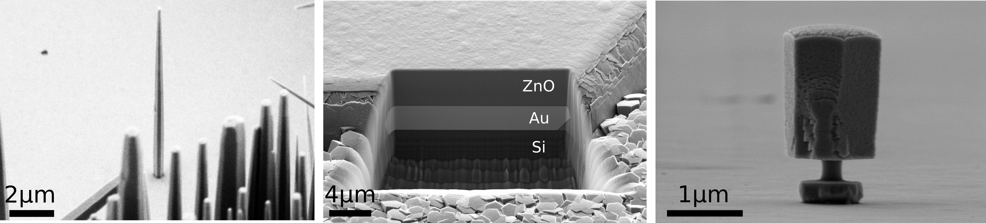
Most often top-down fabrication techniques such as etching and lithography are used in the fabrication of functional nanodevices. In contrast, pre-patterning of a substrate which results in the selective growth of a material can be very advantageous due less process complexity and process induced damage. In our work, we fabricate removable molds in either photoresist or PMMA using top-down fabrication techniques which we then grow through using a bottom-up, low temperature, aqueous growth of single crystalline ZnO. We investigate the effects of constraining the growth of ZnO in different size and shape molds. Structures are grown for various lengths of time and at different solution concentrations. By varying the different parameters we can create numerous size and shape structures such as those with a very distinct undercut. Electron backscatterer diffraction (EBSD) is also used to investigate the effect that constraining the ZnO growth has on the crystalline structure.
Epitaxial Growth
The interface between metal and oxide or metal and semiconductor can play a critical role in the performance of electrical and optical devices. Most metal-oxide interfaces are formed using vapor phase deposition techniques which do not result in an epitaxial relationship. The low temperature aqueous growth method used in our group overcomes several of these problems. We have been able to epitaxially grow single crystalline ZnO on single crystalline gold. A number of techniques including electron backscatterer diffraction (EBSD) and transmission electron microscopy (TEM) are used to investigate the epitaxial relationship of the two materials. In addition, scanning electron microscopy (SEM) and atomic force microscopy (AFM) are used to investigate the ZnO morphology after both nucleation and growth. We have found that the speed of the ZnO nucleation (fast nucleation performed in a microwave and slow nucleation done in an oven) results in differences in the surface morphology of the material after growth.
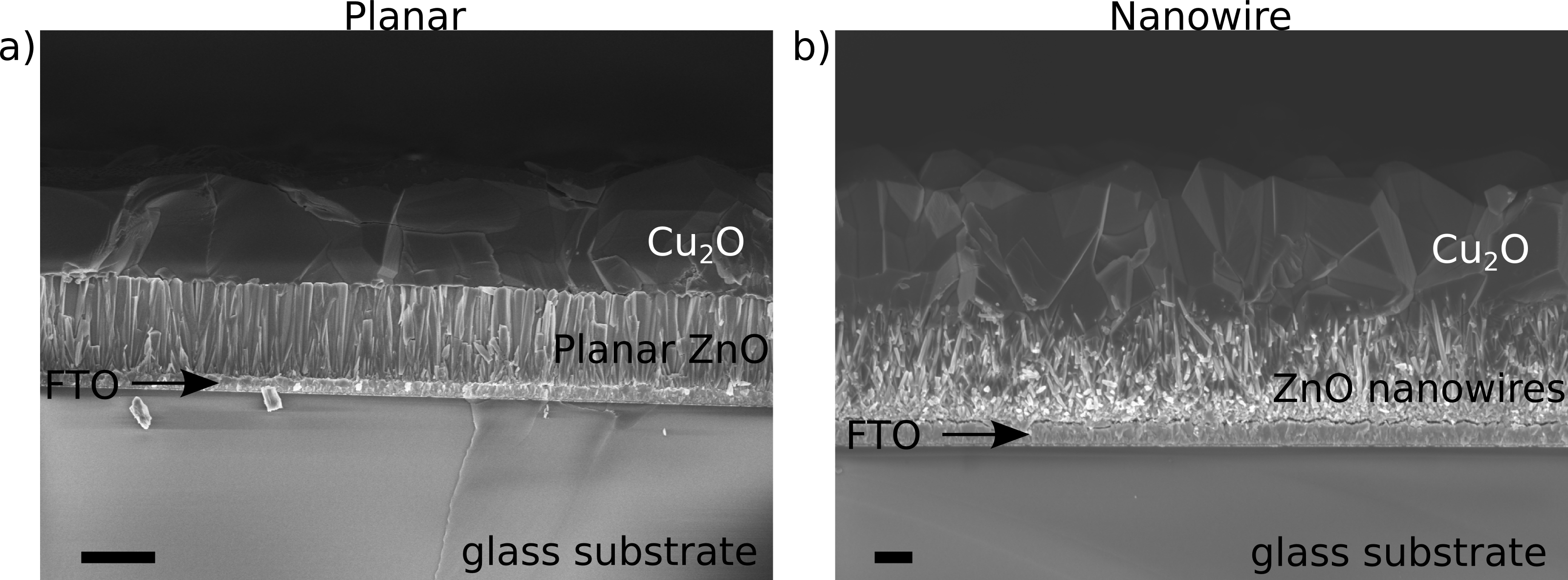
All-oxide photovoltaics
Currently, the most used photovoltaic (solar cell) materials are Si and CdTe (although Si wins in market penetration by a long shot). Although the price of production for these photovoltaics has decreased dramatically in the last decade, continued reduction of the costs for photovoltaics will make its adoption by mass markets more attractive. To this end, we have studied Cu2O/ZnO photovoltaics. In order to increase efficiency of this historic photovoltaic system, we have incorporated nanostructured ZnO into the device.